Study › Amateur Extra › E6C

E6C

CIRCUIT COMPONENTS

Digital ICs: families of digital ICs; gates; programmable logic devices

Drill results are kept in this browser. Log in to keep them on your account and get a study plan.

E6C011 of 11

What is the function of hysteresis in a comparator?

Why A comparator with no hysteresis switches the instant the input crosses a single threshold, so a noisy signal hovering near that point makes the output chatter back and forth. Hysteresis adds a small amount of positive feedback so that the threshold moves after each transition: once the output goes high, the input must fall to a lower level before it switches back. Those two separate trip points mean noise smaller than the hysteresis gap cannot flip the output, giving one clean transition.
Watch out The claim about increased sensitivity is backwards. Hysteresis deliberately makes the comparator less sensitive near the switching point, which is exactly what buys the noise immunity.
Hysteresis = two thresholds with a dead zone between them, so noise can't make the output chatter.
HamSandwich explanation, first draft. The question and answers are the NCVEC text.
E6C022 of 11

What happens when the level of a comparator's input signal crosses the threshold voltage?

Why A comparator continuously compares its input voltage against a reference (threshold) voltage using very high open-loop gain. As soon as the input passes that reference, even by a millivolt, the huge gain drives the output to one supply rail or the other, so the output flips between its two logic states. That is what makes comparators useful as analog-to-digital threshold detectors, level sensors and squaring circuits.
Watch out The choice about the reference level appearing at the output describes a buffer or voltage follower, not a comparator; a comparator's output is a saturated high or low, not a copy of the reference.
Comparator = one-bit ADC: input above reference, output slams high; below, output slams low.
HamSandwich explanation, first draft. The question and answers are the NCVEC text.
E6C033 of 11

What is tri-state logic?

Why A tri-state output has the usual logic low (0) and logic high (1) drive states plus a third condition in which the output transistors are all turned off, presenting a high impedance that effectively disconnects the pin from the line. That lets many devices share a common bus: only the one device whose output-enable is asserted drives the bus while the rest float in high-Z. The third 'state' is an electrical condition, not an extra logic level.
Watch out The ternary math choice misreads 'tri-state' as a three-valued number system, and the impedance matching answer confuses a digital enable function with analog load matching; bus drivers do not tune themselves to the load.
Three states = 0, 1, and off (high-Z). The third one is 'disconnected', not a third logic level.
HamSandwich explanation, first draft. The question and answers are the NCVEC text.
E6C044 of 11

Which of the following is an advantage of BiCMOS logic?

Why BiCMOS puts CMOS and bipolar transistors on the same die so each does what it does best. The CMOS input stage gives very high input impedance, so it barely loads the driving circuit, while bipolar output transistors provide low output impedance and high current drive for fast switching of capacitive loads. You get CMOS's low static power at the input together with bipolar's drive strength at the output.
Watch out The cost claim is backwards: fabricating both device types on one chip takes extra mask steps, so BiCMOS is more complex and more expensive than plain CMOS. And the CMOS gate inputs still have thin oxide, so BiCMOS is just as vulnerable to static discharge.
BiCMOS = best of Bi and CMOS: CMOS in (high Z), bipolar out (low Z, big drive).
HamSandwich explanation, first draft. The question and answers are the NCVEC text.
E6C055 of 11

Which of the following digital logic families has the lowest power consumption?

Why CMOS (complementary metal-oxide semiconductor) uses matched pairs of P-channel and N-channel MOSFETs so that in either stable logic state one transistor of the pair is off, leaving essentially no DC path from supply to ground. Current is drawn mainly during switching transitions, to charge and discharge capacitance, so static power consumption is extremely low. That is why CMOS dominates battery-powered and large-scale digital designs.
Watch out ECL is the opposite extreme: its transistors are kept in the active region and never saturate, which makes it the fastest but the most power-hungry family. TTL variants, including Schottky, draw steady bias current through their input and output stages, and NMOS logic conducts through a pull-up load whenever the output is low.
CMOS = Complementary pairs, so one is always off: near-zero idle current. ECL is fastest but thirstiest.
HamSandwich explanation, first draft. The question and answers are the NCVEC text.
E6C066 of 11

Why do CMOS digital integrated circuits have high immunity to noise on the input signal or power supply?

Why CMOS logic inputs switch state when the input passes roughly 50% of the supply rail (Vdd/2), so a logic low can drift upward by nearly half the supply and a logic high can droop by nearly half before the gate misreads it. That symmetric, wide noise margin on both the high and low sides is what gives CMOS its noise immunity, and because the threshold tracks the supply, supply variation shifts the threshold along with the signal levels. By contrast, TTL thresholds sit near 1.4 V on a 5 V rail, leaving much less margin on the low side.
Watch out The claim that the threshold is about twice the supply voltage is impossible, since no input driven from the same supply could ever reach that level and the gate would never switch. Bypass capacitance is added externally, not inherent, and limited bandwidth is not why CMOS resists noise.
CMOS switches at half the rail: about half the supply of noise margin on each side.
HamSandwich explanation, first draft. The question and answers are the NCVEC text.
E6C077 of 11

What best describes a pull-up or pull-down resistor?

Why Digital inputs are high impedance, so if nothing actively drives them they float and pick up noise, reading randomly high or low. A pull-up resistor ties the line to V+ and a pull-down ties it to ground, so the line sits at a defined logic level whenever the driving device is open circuit (for example a switch that is not closed, or an open-collector/open-drain output). Typical values are a few kilohms: high enough not to waste current, low enough to overcome leakage and noise.
Watch out The key-click choice describes RC shaping of a CW keying waveform, which is a transmitter filtering issue and has nothing to do with defining a logic level on a floating line.
Pull-up/pull-down = give a floating input a home. Up to V+, down to ground.
HamSandwich explanation, first draft. The question and answers are the NCVEC text.
E6C088 of 11

In Figure E6-3, which is the schematic symbol for a NAND gate?
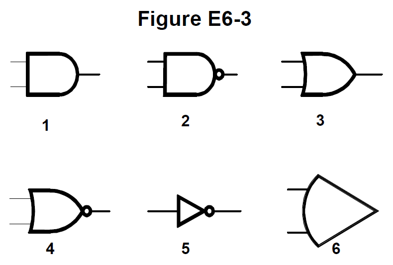
Figure E6-3 from the NCVEC question pool
Why A NAND gate is simply an AND gate followed by an inverter, so its symbol is the AND body, a flat back with a half-round or D-shaped front, plus a small bubble (circle) at the output that means inversion. Symbol 2 in Figure E6-3 has that D-shaped AND body with the inverting bubble, so it is the NAND. Its output is low only when all inputs are high, the exact complement of AND.
Watch out Symbol 1 is the same D-shaped body without the output bubble, which is a plain AND gate; the curved, shield-shaped bodies in the figure are the OR family.
Shape tells AND vs OR (D = AND, shield = OR); bubble on the output adds the N in NAND/NOR.
HamSandwich explanation, first draft. The question and answers are the NCVEC text.
E6C099 of 11

What is used to design the configuration of a field-programmable gate array (FPGA)?

Why An FPGA is a chip full of uncommitted logic blocks and routing that you configure into whatever circuit you want. Designers describe the desired logic behavior in a hardware description language such as VHDL or Verilog, and synthesis tools compile that description into the bitstream that configures the gates and interconnects. HDL is text that describes parallel hardware structure and timing, not a sequence of instructions for a processor.
Watch out Machine and assembly language is tempting because it is also low-level code, but that programs a CPU's instruction execution, not the physical logic fabric of an FPGA. Karnaugh maps are a manual technique for simplifying small Boolean expressions, and an auto-router places traces on a printed circuit board.
FPGA = HDL. Think VHDL/Verilog: you describe the hardware, you don't write instructions for it.
HamSandwich explanation, first draft. The question and answers are the NCVEC text.
E6C1010 of 11

In Figure E6-3, which is the schematic symbol for a NOR gate?

Figure E6-3 from the NCVEC question pool
Why A NOR gate is an OR gate followed by an inversion, so its symbol is the OR shape, a body with a concave curved back and a pointed, bullet-like nose, with a small inversion bubble on the output. The bubble is what makes it NOR rather than plain OR: the output is low whenever any input is high, and high only when all inputs are low. In Figure E6-3 that pointed-nose-plus-bubble symbol is the one numbered 4.
Watch out The most tempting mistake is the NAND symbol, which also has an output bubble but uses the AND body: a flat back and a smooth semicircular (D-shaped) front instead of the pointed OR nose.
Bubble on the output = NOT. D-shape = AND, pointed nose = OR. Pointed nose + bubble = NOR.
HamSandwich explanation, first draft. The question and answers are the NCVEC text.
E6C1111 of 11

In Figure E6-3, which is the schematic symbol for the NOT operation (inversion)?

Figure E6-3 from the NCVEC question pool
Why The NOT gate, or inverter, is drawn as a plain triangle pointing at its output with a small circle (bubble) at the tip. The triangle alone is a buffer; the bubble is what says "invert," so the output is the logical complement of the single input. Unlike every other gate in the figure, it has only one input, which is the quickest way to spot it. In Figure E6-3 that symbol is number 5.
Watch out The other numbered symbols are two-input gates: AND and NAND use the flat-backed D shape, OR and NOR use the curved shield shape, and the ones with bubbles on their outputs (NAND, NOR) are inverted versions of two-input functions, not simple inversion.
One input, triangle plus bubble equals NOT. Bubble always means invert; count the inputs to tell NOT from NAND/NOR.
HamSandwich explanation, first draft. The question and answers are the NCVEC text.
Nagoya NA-771 Dual Band Handheld AntennaSponsored · View on Amazon →BaoFeng BF-F8HP 8W Dual Band HandheldSponsored · View on Amazon →
← E6B All groups E6D →