G7A09
PRACTICAL CIRCUITS · - Power supplies; schematic symbols
G7A09G7A →
Which symbol in figure G7-1 represents a field effect transistor?
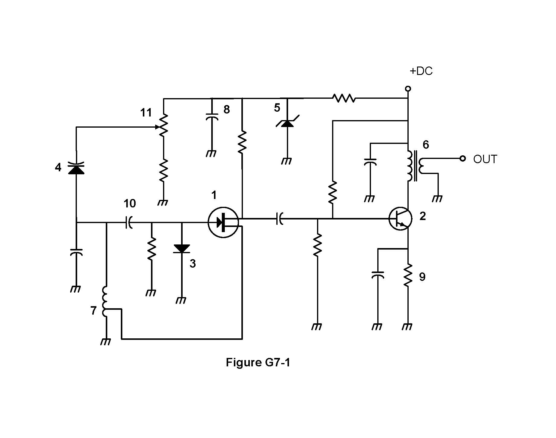
- ASymbol 2
- BSymbol 5
- CSymbol 1
- DSymbol 4
Why A field effect transistor is drawn as a straight channel line with the source and drain leads coming off it at right angles, and a separate gate lead that meets the channel with an arrow on the gate. The three leads are gate, drain and source, and the gate does not touch the channel electrically, which is why the symbol shows it as a separate bar. Symbol 1 in Figure G7-1 has this gate-to-channel layout, so it is the FET.
Watch out The bipolar junction transistor symbols are the tempting ones: they show a base bar with the emitter and collector angling off it and the arrow on the emitter, not on the control lead. One of the other choices is a Zener diode, recognizable by the bent or flag-shaped cathode bar.
FET: arrow is on the gate and the leads meet the channel at right angles. BJT: arrow is on the slanted emitter.
HamSandwich explanation, first draft. The question and answers are the NCVEC text.
The rest of G7A
- G7A01 What is the function of a power supply bleeder resistor?
- G7A02 Which of the following components are used in a power supply filter network?
- G7A03 Which type of rectifier circuit uses two diodes and a center-tapped transformer?
- G7A04 What is characteristic of a half-wave rectifier in a power supply?
- G7A05 What portion of the AC cycle is converted to DC by a half-wave rectifier?
- G7A06 What portion of the AC cycle is converted to DC by a full-wave rectifier?
- G7A07 What is the output waveform of an unfiltered full-wave rectifier connected to a resistive load?
- G7A08 Which of the following is characteristic of a switchmode power supply as compared to a linear power supply?
- G7A09 Which symbol in figure G7-1 represents a field effect transistor?
- G7A10 Which symbol in figure G7-1 represents a Zener diode?
- G7A11 Which symbol in figure G7-1 represents an NPN junction transistor?
- G7A12 Which symbol in Figure G7-1 represents a solid core transformer?
- G7A13 Which symbol in Figure G7-1 represents a tapped inductor?