Study › Amateur Extra › E7B

E7B

PRACTICAL CIRCUITS

Amplifiers: class of operation; vacuum tube and solid-state circuits; distortion and intermodulation; spurious and parasitic suppression; switching-type amplifiers

Drill results are kept in this browser. Log in to keep them on your account and get a study plan.

E7B011 of 12

For what portion of the signal cycle does each active element in a push-pull, Class AB amplifier conduct?

Why Amplifier classes are defined by conduction angle, the portion of the input cycle during which the device conducts. Class A conducts the full 360 degrees, Class B exactly 180 degrees, and Class C less than 180. Class AB sits between A and B, so each device is biased slightly into conduction and stays on for more than 180 but less than 360 degrees, which reduces the crossover distortion a pure Class B push-pull stage would show.
Watch out Exactly 180 degrees describes Class B, and the entire cycle describes Class A; the "AB" name is the clue that it falls between those two.
A=360, B=180, C=under 180, so AB is between 180 and 360.
HamSandwich explanation, first draft. The question and answers are the NCVEC text.
E7B022 of 12

What is a Class D amplifier?

Why A Class D amplifier does not operate its devices in the linear region at all; the transistors are driven fully on or fully off like switches, usually from a pulse-width-modulated drive signal, and a low-pass output filter recovers the desired waveform. Because a switch that is off passes no current and a switch that is on drops almost no voltage, device dissipation is very low and efficiency can exceed 90 percent. The tradeoff is that the raw output is rich in harmonics, so output filtering is essential.
Watch out The description of an amplifier biased for low distortion points to linear classes such as Class A or AB, which are the opposite design philosophy: good linearity paid for with low efficiency. 'Drift-mode FETs' is not a real amplifier class.
D is for Digital-like switching: devices are either fully on or fully off, so efficiency is high and a filter cleans up the output.
HamSandwich explanation, first draft. The question and answers are the NCVEC text.
E7B033 of 12

What circuit is required at the output of an RF switching amplifier?

Why Switching amplifiers (Class D, E and F) drive the active devices fully on or fully off, so the raw output is essentially a square wave rather than a sine wave. A square wave is loaded with harmonics of the operating frequency, so a low-pass or band-pass filter (often a resonant tank) must follow the amplifier to strip those harmonics and leave a clean carrier. Without it the amplifier would violate the spurious emission limits of 97.307 and splatter energy across other bands.
Watch out A high-pass filter is exactly backwards: the problem is energy above the operating frequency, not weak low-frequency response. Load resistors do not belong there either, since a switching amplifier gets its efficiency by delivering all its power to the antenna, not burning it in a resistor.
Switching amp = square wave out; square waves are full of harmonics, so always follow with a low-pass filter.
HamSandwich explanation, first draft. The question and answers are the NCVEC text.
E7B044 of 12

What is the operating point of a Class A common emitter amplifier?

Why Class A means the transistor conducts for the entire 360 degrees of the input cycle, so the quiescent (no-signal) collector current must sit far enough from both extremes that neither peak of the signal clips. On the DC load line, saturation is one end (maximum current, minimum collector voltage) and cutoff is the other (no current, full supply voltage); biasing at roughly the midpoint gives the largest symmetrical output swing and the lowest distortion, at the cost of steady power dissipation and efficiency under about 25-30 percent.
Watch out The idea of sitting halfway between emitter and base voltage confuses the base-emitter junction drop (about 0.7 V in silicon) with the Q-point, which is defined by collector current and collector-emitter voltage on the load line, not by that junction.
Class A = always on: park the Q-point mid-load-line, halfway between saturation and cutoff.
HamSandwich explanation, first draft. The question and answers are the NCVEC text.
E7B055 of 12

What can be done to prevent unwanted oscillations in an RF power amplifier?

Why Unwanted oscillation happens when enough output energy feeds back in phase to the input, usually through the device's internal capacitance (plate-to-grid or drain-to-gate) or through stray lead inductance that resonates at VHF. Neutralization cancels that internal feedback by deliberately coupling a small out-of-phase sample of the output back to the input. Parasitic suppressors, typically a few turns of wire in parallel with a small resistor placed in the plate or drain lead, add loss at VHF where the parasitic resonance occurs while barely affecting the operating frequency.
Watch out Tuning both input and output for maximum power is a normal amplifier adjustment for efficiency and output, but it does nothing about feedback paths and can actually make an unstable stage break into oscillation.
Instability = feedback. Kill it two ways: neutralize the internal capacitance, suppress the VHF parasitic.
HamSandwich explanation, first draft. The question and answers are the NCVEC text.
E7B066 of 12

What is a characteristic of a grounded-grid amplifier?

Why In a grounded-grid (cathode-driven) stage the drive signal is applied to the cathode, which is a low-impedance electrode carrying the full cathode current. That gives a typical input impedance on the order of tens of ohms, which is convenient because it roughly matches 50-ohm coax drive from an exciter. The grid acts as a grounded electrostatic shield between input and output, so the stage is stable without neutralization, but the driving power passes through to the output, so power gain is modest.
Watch out High power gain is the tempting opposite: grounded-grid amplifiers actually have less gain than grounded-cathode designs because the drive power adds to the output rather than being isolated from it.
Grounded grid = cathode driven = low Z in, low gain, no neutralizing needed.
HamSandwich explanation, first draft. The question and answers are the NCVEC text.
E7B077 of 12

Which of the following is the likely result of using a Class C amplifier to amplify a single-sideband phone signal?

Why A Class C stage conducts for less than half of each RF cycle, so its output is a series of current pulses shaped by a tuned tank rather than a faithful copy of the input envelope. SSB is an amplitude-varying (non-constant-envelope) mode, so that envelope information is destroyed, producing severe distortion and splatter well outside the intended channel. Only constant-envelope modes such as CW and FM can tolerate Class C; SSB requires a linear amplifier, Class A, AB, or B.
Watch out The choices about reduced intermodulation or better intelligibility describe what a linear amplifier gives you; Class C does the opposite, generating strong intermodulation products and splatter.
Class C = constant-envelope only (CW/FM). Feed it SSB and you get splatter.
HamSandwich explanation, first draft. The question and answers are the NCVEC text.
E7B088 of 12

Why are switching amplifiers more efficient than linear amplifiers?

Why Power dissipated in the active device is the product of the voltage across it and the current through it. A switching amplifier (Class D, E or F) drives the transistor hard between full conduction (saturation, so very low voltage across it) and cutoff (essentially no current through it), and in both states that V x I product is nearly zero. Only the brief transitions between states waste power, so efficiencies of 90 percent or more are possible, versus roughly 25 to 66 percent for linear Class A, AB or B stages where the device sits at intermediate voltage and current.
Watch out High operating voltage has nothing to do with it; a linear amplifier at any supply voltage still dissipates heat because the device spends its time partly on. The harmonic content comment is backwards too, since switching amplifiers generate lots of harmonics and need heavy output filtering.
Efficiency comes from P = V x I being near zero: full on means no volts, full off means no amps.
HamSandwich explanation, first draft. The question and answers are the NCVEC text.
E7B099 of 12

What is characteristic of an emitter follower (or common collector) amplifier?

Why In a common collector (emitter follower) stage the load sits in the emitter leg, so the emitter voltage tracks the base voltage about 0.7 V below it. The output therefore follows the input with voltage gain just under 1 and no phase reversal, giving in-phase input and output. Its value is impedance transformation: high input impedance, low output impedance, and useful current gain, which makes it a good buffer or driver stage.
Watch out The choice pairing low input impedance with phase inversion mixes up two other configurations: the common emitter inverts the signal, and the common base is the one with low input impedance and no inversion. Differential inputs describe an op amp or long-tailed pair, and the OR-circuit answer is digital logic, not an analog amplifier stage.
Emitter follower: the emitter FOLLOWS the base, so it stays in phase, gain about 1, high Z in, low Z out.
HamSandwich explanation, first draft. The question and answers are the NCVEC text.
E7B1010 of 12

In Figure E7-1, what is the purpose of R1 and R2?
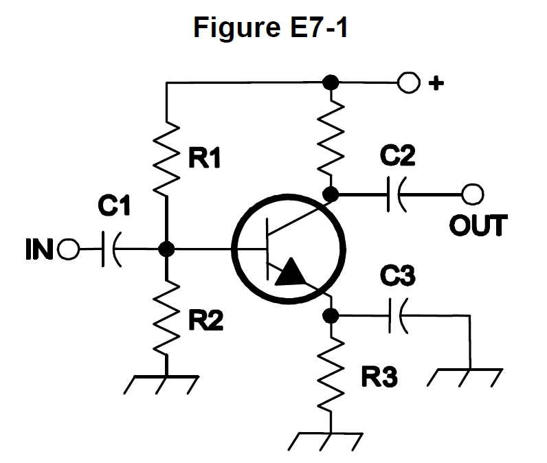
Figure E7-1 from the NCVEC question pool
Why In Figure E7-1 the two resistors run from the supply rail to ground with their junction tied to the transistor's base. That divider sets a fixed DC voltage at the base, which (minus the roughly 0.7 V base-emitter drop) sets the emitter voltage and therefore the quiescent collector current. This is the classic voltage divider bias network used to place a transistor stage at a stable operating point that does not drift much with temperature or beta.
Watch out Self bias describes a scheme where the device's own current through an emitter or cathode resistor develops the bias voltage, not a divider off the supply; load resistors would be in the collector or output path, developing the signal output voltage.
Two resistors in series across the supply, tap to the base: divider = bias. R1/R2 in E7-1 is always voltage divider bias.
HamSandwich explanation, first draft. The question and answers are the NCVEC text.
E7B1111 of 12

In Figure E7-1, what is the purpose of R3?

Figure E7-1 from the NCVEC question pool
Why R3 sits in the emitter leg of the transistor. Collector/emitter current flowing through it develops a voltage drop that raises the emitter above ground, which subtracts from the base-emitter forward bias. If the transistor starts to conduct harder (from heat or device variation), the larger drop across R3 pulls the bias back down, so the stage sets and stabilizes its own operating point. That degenerative action is what is meant by self bias, also called emitter bias.
Watch out Fixed bias is what the base voltage divider supplies, and emitter bypass is the job of the capacitor placed across R3 to keep the resistor from reducing AC gain.
Resistor in the emitter leg = self bias; the capacitor across it = bypass; the divider on the base = fixed bias.
HamSandwich explanation, first draft. The question and answers are the NCVEC text.
E7B1212 of 12

What type of amplifier circuit is shown in Figure E7-1?

Figure E7-1 from the NCVEC question pool
Why You name a transistor stage by the element that is common to both the input and the output loops at signal frequency. In Figure E7-1 the signal enters at the base, leaves at the collector, and the emitter sits at AC ground (grounded directly or through a bypass capacitor), so the emitter is the common element. This configuration gives both voltage and current gain and inverts the signal 180 degrees.
Watch out Common collector and emitter follower are two names for the same circuit, so neither can be the answer here; in that circuit the output is taken from the emitter and the voltage gain is slightly less than one. A common base stage would drive the emitter and hold the base at AC ground.
Follow the output: from the collector = common emitter, from the emitter = follower. Also, two choices naming the same circuit are both wrong.
HamSandwich explanation, first draft. The question and answers are the NCVEC text.
Yaesu FT-65R VHF/UHF Dual Band HandheldSponsored · View on Amazon →Baofeng BF-F8HP Pro Dual Band HandheldSponsored · View on Amazon →
← E7A All groups E7C →