E6A11
CIRCUIT COMPONENTS · Semiconductor materials and devices: semiconductor materials; bipolar junction transistors; operation and types of field-effect transistors
E6A11E6A →
In Figure E6-1, which is the schematic symbol for a P-channel junction FET?
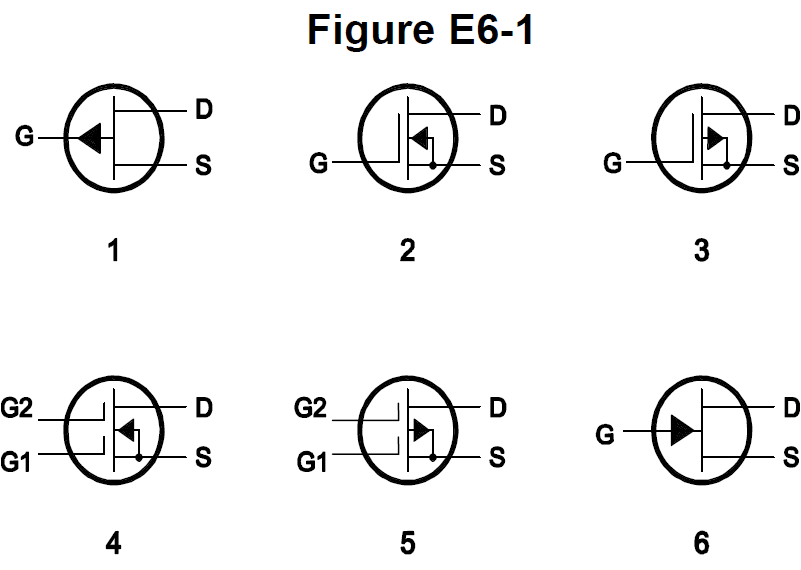
- A1
- B2
- C3
- D6
Why A junction FET symbol shows the channel as a straight line between source and drain with a gate arrow touching it, and the arrow is just the gate-channel PN junction diode. Since a diode arrow points from P material toward N material, a P-channel JFET has an N-type gate, so the arrow points outward, away from the channel line. Symbol 1 in Figure E6-1 is the JFET whose gate arrow points away from the channel, making it the P-channel device.
Watch out Symbol 2 is the same JFET outline but with the gate arrow pointing in toward the channel, which is the N-channel version; the other listed symbols are MOSFET or bipolar devices.
N-channel points iN. Arrow toward the channel = N-channel, arrow away = P-channel.
HamSandwich explanation, first draft. The question and answers are the NCVEC text.
The rest of E6A
- E6A01 In what application is gallium arsenide used as a semiconductor material?
- E6A02 Which of the following semiconductor materials contains excess free electrons?
- E6A03 Why does a PN-junction diode not conduct current when reverse biased?
- E6A04 What is the name given to an impurity atom that adds holes to a semiconductor crystal structure?
- E6A05 How does DC input impedance at the gate of a field-effect transistor (FET) compare with that of a bipolar tra…
- E6A06 What is the beta of a bipolar junction transistor?
- E6A07 Which of the following indicates that a silicon NPN junction transistor is biased on?
- E6A08 What is the term for the frequency at which the grounded-base current gain of a bipolar junction transistor h…
- E6A09 What is a depletion-mode field-effect transistor (FET)?
- E6A10 In Figure E6-1, which is the schematic symbol for an N-channel dual-gate MOSFET?
- E6A11 In Figure E6-1, which is the schematic symbol for a P-channel junction FET?
- E6A12 What is the purpose of connecting Zener diodes between a MOSFET gate and its source or drain?