Study › Amateur Extra › E6A

E6A

CIRCUIT COMPONENTS

Semiconductor materials and devices: semiconductor materials; bipolar junction transistors; operation and types of field-effect transistors

Drill results are kept in this browser. Log in to keep them on your account and get a study plan.

E6A011 of 12

In what application is gallium arsenide used as a semiconductor material?

Why Gallium arsenide has much higher electron mobility than silicon, so carriers cross the device faster and it can amplify or switch at far higher frequencies with less noise. That makes GaAs the material of choice for microwave devices such as GaAs FETs, low-noise preamplifiers and monolithic microwave integrated circuits. Its semi-insulating substrate also cuts stray capacitance and loss at GHz frequencies.
Watch out High-current rectifiers and high-power audio stages are silicon (or silicon carbide) territory, where GaAs offers no advantage and costs far more; low-frequency RF is easily handled by ordinary silicon devices.
GaAs = Gigahertz Amplifier stuff. Think microwave preamp, not power rectifier.
HamSandwich explanation, first draft. The question and answers are the NCVEC text.
E6A022 of 12

Which of the following semiconductor materials contains excess free electrons?

Why Pure silicon or germanium is doped with impurity atoms to change its conduction. Adding a donor impurity with five valence electrons (phosphorus, arsenic, antimony) leaves one electron per atom with no bond to fill, so the majority carriers are free electrons. That material is called N-type because the mobile charge carriers are Negative.
Watch out P-type is the opposite: it is doped with a trivalent acceptor such as boron or indium, leaving holes (missing electrons) as the majority carrier. Bipolar and insulated gate are transistor construction terms, not semiconductor material types.
N = Negative carriers = free electrons; P = Positive carriers = holes.
HamSandwich explanation, first draft. The question and answers are the NCVEC text.
E6A033 of 12

Why does a PN-junction diode not conduct current when reverse biased?

Why In a PN junction the majority carriers are holes on the P side and electrons on the N side. Reverse bias puts the negative supply terminal on the P material and positive on the N, pulling both kinds of carrier away from the junction. That leaves a wider carrier-free depletion region with no mobile charge to carry current, so only a tiny leakage current flows. Forward bias does the opposite: it pushes carriers toward the junction, narrowing the depletion region until conduction begins.
Watch out The idea that holes and electrons combine and turn the whole diode into an insulator is wrong because only the thin junction region is depleted; the bulk P and N material is still full of carriers and conducts fine, and the diode conducts normally as soon as the bias is reversed.
Reverse bias pulls carriers apart: wide depletion region = no current. Forward bias squeezes it shut = current flows.
HamSandwich explanation, first draft. The question and answers are the NCVEC text.
E6A044 of 12

What is the name given to an impurity atom that adds holes to a semiconductor crystal structure?

Why Doping a silicon crystal with a trivalent element such as boron, gallium or indium leaves one bonding site short of an electron. That vacancy is a hole, and because the impurity atom readily accepts an electron from a neighboring bond, it is called an acceptor impurity. Acceptor doping produces P-type material, where holes are the majority carriers.
Watch out A donor impurity is the opposite case: a pentavalent atom like phosphorus or arsenic donates an extra free electron and creates N-type material. 'N-type impurity' points at that same electron-adding side of the story.
Acceptor Accepts electrons, so it Adds holes = P-type. Donor Donates electrons = N-type.
HamSandwich explanation, first draft. The question and answers are the NCVEC text.
E6A055 of 12

How does DC input impedance at the gate of a field-effect transistor (FET) compare with that of a bipolar transistor?

Why An FET is a voltage-controlled device: the gate is either insulated from the channel by an oxide layer (MOSFET) or is a reverse-biased junction (JFET), so essentially no DC gate current flows and the DC input impedance is very high, often megohms or more. A bipolar transistor is current-controlled, with a forward-biased base-emitter junction that must draw base current, giving an input impedance of only hundreds of ohms to a few kilohms. So the FET gate presents the much higher DC input impedance.
Watch out The choice saying both are high is tempting because BJT amplifier stages can be designed for fairly high impedance with emitter degeneration, but the device's own forward-biased base junction is inherently low impedance.
FET gate = voltage control, almost no current in, so high Z. BJT base = current control, so low Z.
HamSandwich explanation, first draft. The question and answers are the NCVEC text.
E6A066 of 12

What is the beta of a bipolar junction transistor?

Why Beta (also written hFE) is the current gain of a bipolar junction transistor: a small base current controls a much larger collector current, and beta is the ratio of the change in collector current to the change in base current. Typical small-signal transistors have betas of roughly 50 to 300, so 1 mA of base current might support 100 mA of collector current. It is related to alpha (collector current divided by emitter current) by beta = alpha / (1 - alpha).
Watch out The choice about the frequency where gain drops to 0.707 describes a cutoff or corner frequency such as the alpha cutoff, not beta itself; breakdown voltage and switching speed are separate device ratings.
Beta = Base current boosted: collector current divided by base current.
HamSandwich explanation, first draft. The question and answers are the NCVEC text.
E6A077 of 12

Which of the following indicates that a silicon NPN junction transistor is biased on?

Why The base-emitter junction of a bipolar transistor is just a PN diode, and a forward-biased silicon junction sits at roughly 0.6 to 0.7 volts once it conducts. So measuring about 0.65 V from base to emitter (base positive for an NPN) tells you the transistor is turned on and base current is flowing. Germanium devices would show about 0.3 V instead, and the drop changes only slightly with current because the diode curve is so steep.
Watch out The resistance choices are distractors built from the same numbers: a biased junction is a nonlinear device, and an ohmmeter reading of a fraction of an ohm would indicate a shorted junction, not normal operation. The 6 to 7 volt option would destroy a typical base-emitter junction, which reverse breaks down around 5 to 7 volts and is not run forward anywhere near that.
Silicon diode drop 0.7 V, and B-E is a diode: look for VOLTS, not ohms, about 0.6 to 0.7.
HamSandwich explanation, first draft. The question and answers are the NCVEC text.
E6A088 of 12

What is the term for the frequency at which the grounded-base current gain of a bipolar junction transistor has decreased to 0.7 of the gain obtainable at 1 kHz?

Why In a bipolar transistor, alpha is the current gain in the grounded-base (common-base) configuration, the ratio of collector current to emitter current. Like any gain, it rolls off at high frequencies, and the point where it has fallen to about 0.7 (the 0.707 or -3 dB point) of its low-frequency value, referenced to 1 kHz, is called the alpha cutoff frequency. It is a useful figure of merit because it indicates roughly the highest frequency at which the device is still useful as an amplifier.
Watch out Beta cutoff frequency is the analogous -3 dB point for beta, the grounded-emitter current gain, and it occurs at a much lower frequency than alpha cutoff; "alpha rejection frequency" is not a real transistor parameter.
Alpha goes with the base grounded, beta with the emitter grounded. Grounded base in the question means alpha cutoff.
HamSandwich explanation, first draft. The question and answers are the NCVEC text.
E6A099 of 12

What is a depletion-mode field-effect transistor (FET)?

Why In a depletion-mode FET the channel between source and drain is physically doped in during manufacture, so it conducts with zero volts on the gate. The gate voltage is then used to deplete (pinch off) that existing channel and reduce current, which is why it is called depletion mode. Most JFETs work this way, and depletion-mode MOSFETs exist too; they are described as 'normally on' devices.
Watch out The choice saying there is no current with zero gate voltage describes an enhancement-mode FET, which is normally off and needs gate bias to create (enhance) a channel. The mention of high electron mobility with no holes describes a HEMT, and majority-carrier holes just describes a P-channel device.
Depletion = normally ON, gate voltage takes current away. Enhancement = normally OFF, gate voltage builds the channel.
HamSandwich explanation, first draft. The question and answers are the NCVEC text.
E6A1010 of 12

In Figure E6-1, which is the schematic symbol for an N-channel dual-gate MOSFET?
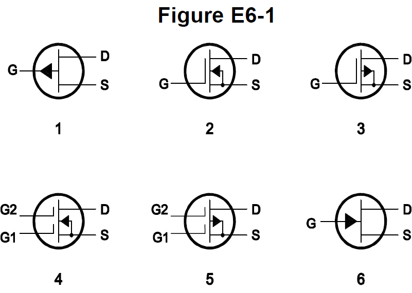
Figure E6-1 from the NCVEC question pool
Why A dual-gate MOSFET symbol shows two separate gate leads drawn as short bars that do not touch the channel line, since the gates are insulated from the channel by an oxide layer. Channel polarity is read from the substrate (body) arrow: on an N-channel device the arrow points inward, toward the channel; on a P-channel device it points outward. Symbol 4 is the one with two insulated gate bars and the inward-pointing substrate arrow, so it is the N-channel dual-gate MOSFET.
Watch out The other dual-gate symbol in the figure is the same device drawn with the substrate arrow reversed, which makes it the P-channel version; symbols with the gate touching the channel line are JFETs, not MOSFETs.
Two floating gate bars = dual-gate MOSFET; arrow poiNting iN = N-channel.
HamSandwich explanation, first draft. The question and answers are the NCVEC text.
E6A1111 of 12

In Figure E6-1, which is the schematic symbol for a P-channel junction FET?

Figure E6-1 from the NCVEC question pool
Why A junction FET symbol shows the channel as a straight line between source and drain with a gate arrow touching it, and the arrow is just the gate-channel PN junction diode. Since a diode arrow points from P material toward N material, a P-channel JFET has an N-type gate, so the arrow points outward, away from the channel line. Symbol 1 in Figure E6-1 is the JFET whose gate arrow points away from the channel, making it the P-channel device.
Watch out Symbol 2 is the same JFET outline but with the gate arrow pointing in toward the channel, which is the N-channel version; the other listed symbols are MOSFET or bipolar devices.
N-channel points iN. Arrow toward the channel = N-channel, arrow away = P-channel.
HamSandwich explanation, first draft. The question and answers are the NCVEC text.
E6A1212 of 12

What is the purpose of connecting Zener diodes between a MOSFET gate and its source or drain?

Why A MOSFET gate is separated from the channel by an extremely thin silicon dioxide insulator, and that layer can be punctured by only a few tens of volts. Since the gate draws essentially no current, even the small charge from handling or a nearby static discharge can build up enough voltage to destroy it. Back-to-back Zener diodes built in from gate to source (or drain) conduct once the voltage reaches their breakdown value, clamping the gate at a safe level and bleeding the static charge away. The tradeoff is a small amount of added leakage and input capacitance, which is why some RF MOSFETs omit them.
Watch out The choice about keeping gate voltage in spec to prevent overheating is close but misses the point: the failure mode being prevented is instantaneous dielectric puncture of the gate oxide, not thermal runaway. The reverse-bias voltage reference idea describes how a Zener is used in a regulator, not here.
Thin gate oxide plus static equals dead FET. Internal Zeners are the MOSFET's lightning arrestor.
HamSandwich explanation, first draft. The question and answers are the NCVEC text.
Tram 1481 Dual Band Base AntennaSponsored · View on Amazon →RG-213 Coax Cable 75ft with PL259 ConnectorsSponsored · View on Amazon →
← E5D All groups E6B →